Currently, both narrow-bandgap and wide-bandgap PSCs are already being independently developed within the KPV-Lab and high-efficiency baseline processes are available for these devices. In this project, we are addressing the challenge of how to integrate both technologies into monolithic perovskite/perovskite tandem solar cells as shown below.
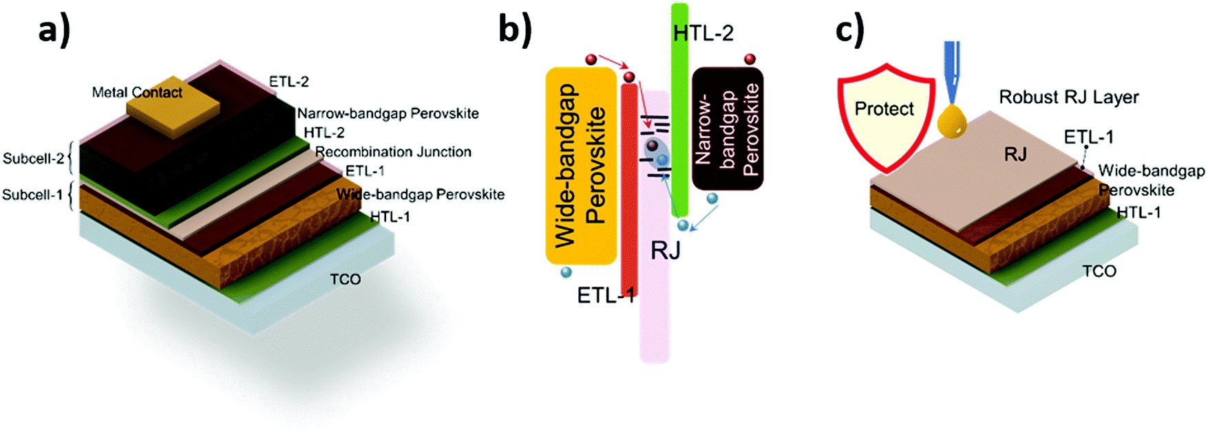
Schematic diagram illustrating the 2T-monolithic all-perovskite tandem structure (a), a sketch of the energy level diagram (b), and the functional role of recombination junctions in these devices (c).
Specific points of attention for this are:
(1) The fabrication of semitransparent wide-bandgap PSCs, requiring the deposition of transparent contact stacks onto the perovskite films. To this end, broadband transparent conductive oxides, electron-transport layers, and hole-transport layers have been explored and integrated into our devices, with specific attention to processing compatibility of all layers.
(2) Exploration of efficient and highly transparent recombination junctions. This is required for effective recombination of holes and electrons that are extracted from the individual sub-cells. Besides, the recombination junction needs to be highly transparent, particularly in the red and near-infrared (NIR) range, to allow this portion of the solar spectrum to be absorbed in the narrow-bandgap sub-cell.
(3) Deposition of narrow-bandgap sub-cells. All perovskite tandem devices are completed by deposition of narrow-bandgap sub-cells on the wide-bandgap perovskite/recombination junction stacks. Here, it is critical to explore orthogonal solution deposition techniques for not damaging the wide-bandgap bottom sub-cell.