support@kaust.edu.sa
+966 (12) 808-3463
  • العربية
logo-black
  • Home
  • People
    • Current
    • Alumni
    • Group photos 
  • Research
  • Publications
    • 2024
    • 2023
    • 2022
    • 2021
    • 2020
    • 2019
    • 2018
    • 2017
    • 2016
    • Journal covers
  • Internship
  • News
  • KPV-LAB in the press
  • Join us
  • Contact us
breadcrumb-bg

Mitigating Plasmonic Absorption Losses at Rear Electrodes in High‐Efficiency Silicon Solar Cells Using Dopant‐Free Contact Stacks

  1. Home
  2. Publications
  • Clear filters

Mitigating Plasmonic Absorption Losses at Rear Electrodes in High‐Efficiency Silicon Solar Cells Using Dopant‐Free Contact Stacks

by Sihua Zhong, Julie Dreon, Quentin Jeangros, Erkan Aydin, Stefaan De Wolf, Fan Fu, Mathieu Boccard, Christophe Ballif
Full Paper Year: 2019 DOI: https://doi.org/10.1002/adfm.201907840

Bibliography

Zhong, S., Dreon, J., Jeangros, Q., Aydin, E., De Wolf, S., Fu, F., Boccard, M., Ballif, C., Mitigating Plasmonic Absorption Losses at Rear Electrodes in High‐Efficiency Silicon Solar Cells Using Dopant‐Free Contact Stacks. Adv. Funct. Mater. 2019, 1907840.
Abstract

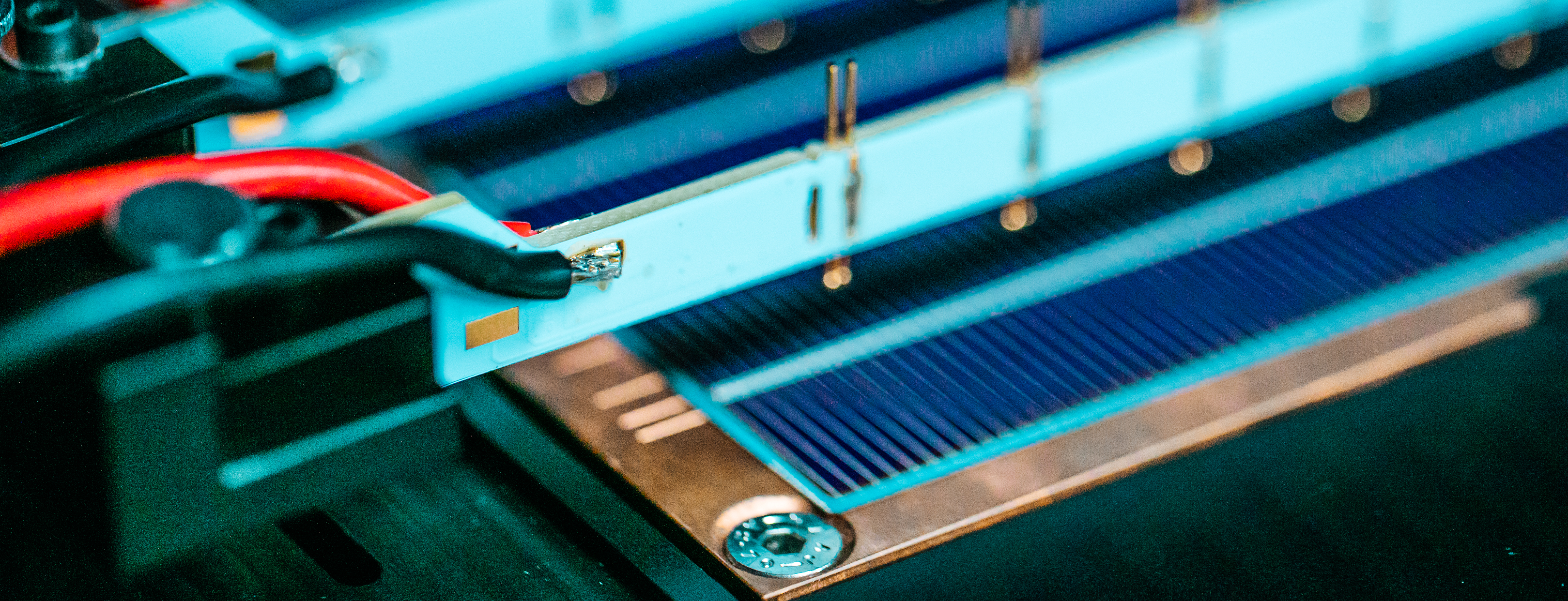
Although charge‐carrier selectivity in conventional crystalline silicon (c‐Si) solar cells is usually realized by doping Si, the presence of dopants imposes inherent performance limitations due to parasitic absorption and carrier recombination. The development of alternative carrier‐selective contacts, using non‐Si electron and hole transport layers, has the potential to overcome such drawbacks and simultaneously reduce the cost and/or simplify the fabrication process of c‐Si solar cells. Nevertheless, devices relying on such non‐Si contacts with power conversion efficiencies (PCEs) that rival their classical counterparts are yet to be demonstrated. In this study, one key element is brought forward toward this demonstration by incorporating low‐pressure chemical vapor deposited ZnO as the electron transport layer in c‐Si solar cells. Placed at the rear of the device, it is found that rather thick (75 nm) ZnO film capped with LiFx/Al simultaneously enables efficient electron selectivity and suppression of parasitic infrared absorption. Next, these electron‐selective contacts are integrated in c‐Si solar cells with MoOx‐based hole‐collecting contacts at the device front to realize full‐area dopant‐free‐contact solar cells. In the proof‐of‐concept device, a PCE as high as 21.4% is demonstrated, which is a record for this novel device class and is at the level of conventional industrial solar cells.

Keywords

carrier-selective contact c-Si solar cells dopant-free contacts plasmonic absoprtion ZnO
logo-white

"KAUST shall be a beacon for peace, hope and reconciliation, and shall serve the people of the Kingdom and the world."

King Abdullah bin Abdulaziz Al Saud, 1924 – 2015

Contact Us

    stefaan.dewolf@kaust.edu.sa
  • 4700 King Abdullah University of Science and Technology

    Al-Kindi (building 5), Level 3 Seaside, Right side

    Thuwal 23955-6900

    Kingdom of Saudi Arabia

Tweets by KAUST_KPVLab

© King Abdullah University of Science and Technology. All rights reserved

Privacy Policy
Terms of Use
Loading...