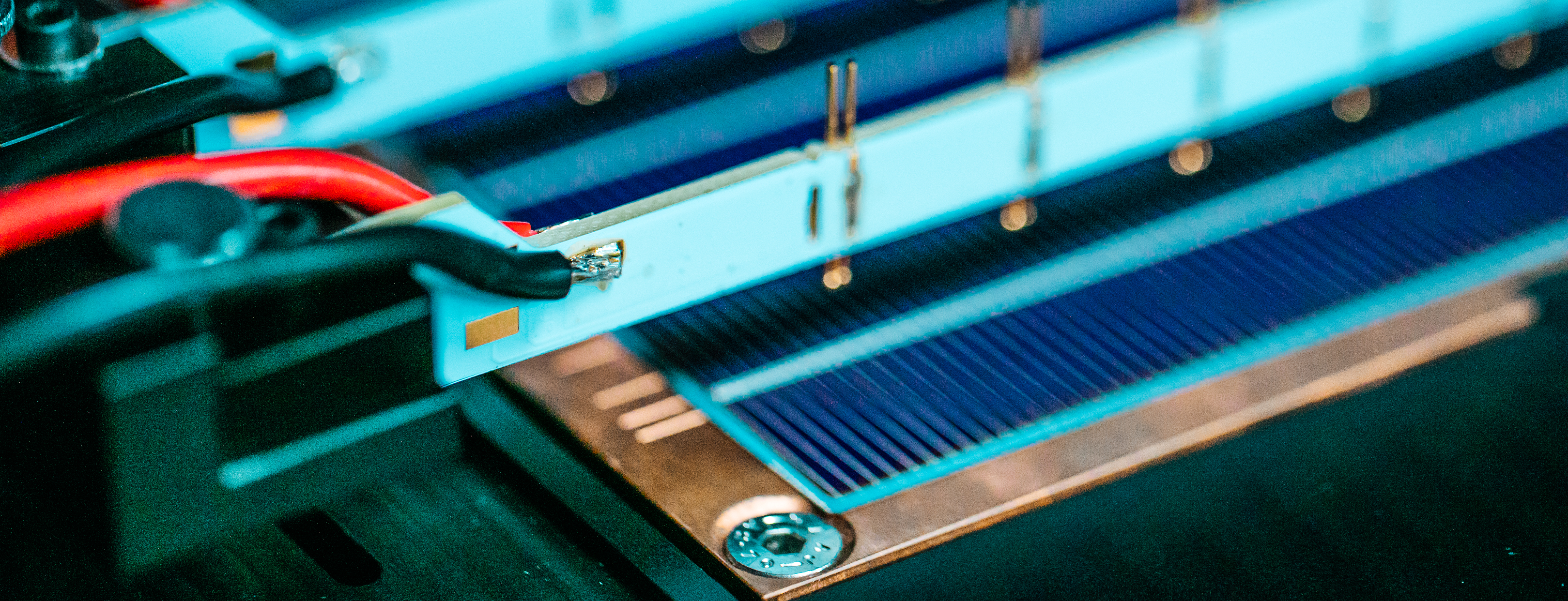
Interdigitated back contact silicon heterojunction solar cells featuring an interband tunnel junction enabling simplified processing
by
B Paviet-Salomon, Andrea Tomasi, D Lachenal, N Badel, Gabriel Christmann, Loris Barraud, Antoine Descoeudres, Jonas Geissbühler, A Faes, Quentin Jeangros, Johannes Peter Seif, Sylvain Nicolay, B Strahm, Stefaan De Wolf, Christophe Ballif, Matthieu Despeisse
Year:
2018
DOI:
https://doi.org/10.1016/j.solener.2018.01.066
Bibliography
Paviet-Salomon, B., A. Tomasi, D. Lachenal, N. Badel, G. Christmann, L. Barraud, A. Descœudres et al. "Interdigitated back contact silicon heterojunction solar cells featuring an interband tunnel junction enabling simplified processing." Solar Energy (2018).