Intrinsic Silicon Buffer Layer Improves Hole‐Collecting Poly‐Si Passivating Contact

by Jingxuan Kang, Wenzhu Liu, Thomas G Allen, Michele De Bastiani, Xinbo Yang, Stefaan De Wolf
Full Paper Year: 2020 DOI: https://doi.org/10.1002/admi.202000188

Bibliography

Kang, J., Liu, W., Allen, T., De Bastiani, M., Yang, X., & De Wolf, S. (2020). Intrinsic Silicon Buffer Layer Improves Hole‐Collecting Poly‐Si Passivating Contact. Advanced Materials Interfaces, 2000188.

Extra Information

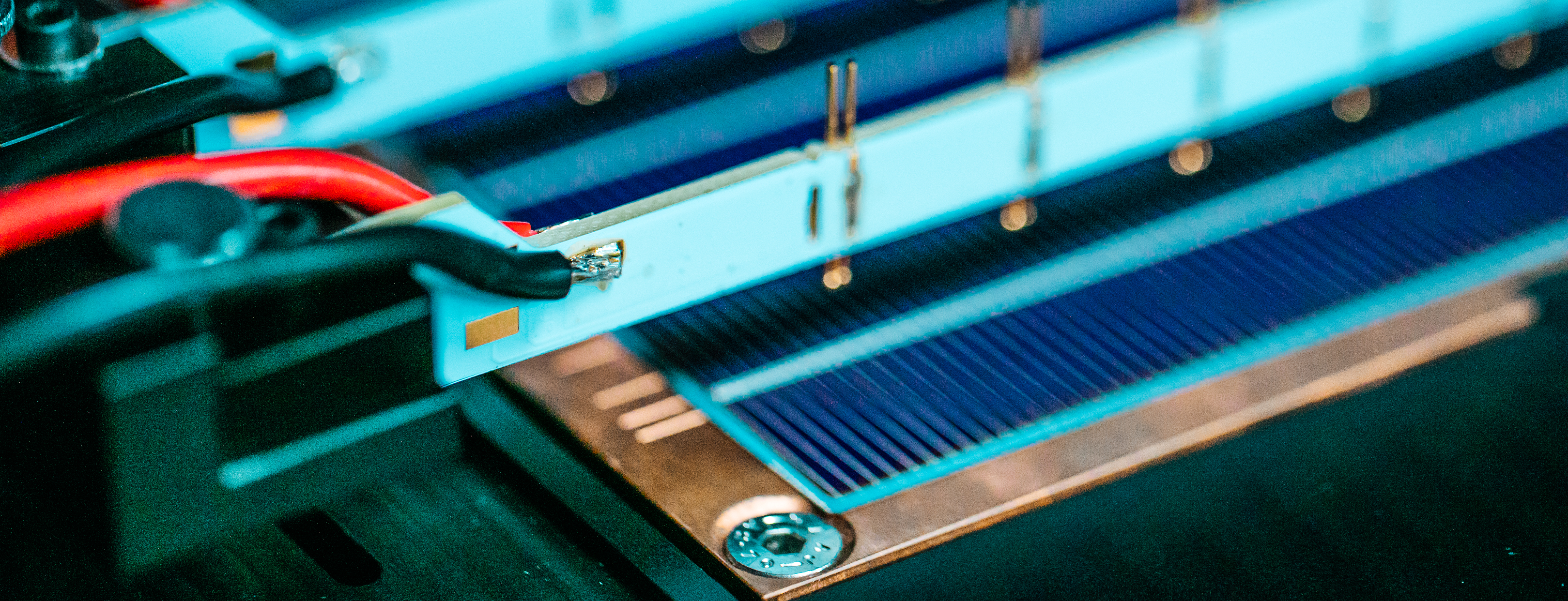
This study, which develops a strategy to circumvent the problem of boron diffusion into the silicon, took place in the recent issue of Advanced Materials Interfaces. This study is the first publication KPV-LAB in the field of poly‐Si passivating contact solar cells.

Abstract

Passivating contacts consisting of doped polycrystalline silicon (poly‐Si) on a thin tunnel‐oxide enable excellent operating voltages for crystalline silicon solar cells. However, hole‐collecting contacts based on boron‐doped poly‐Si do not yet reach their full surface‐passivation potential, likely due to boron diffusion during annealing. In this work, the authors show how the insertion of a thin intrinsic silicon buffer layer between the silicon oxide and poly‐Si is effective in improving the contact passivation. By tailoring the microstructure of the buffer layer, the chemical passivation and contact resistivity are simultaneously significantly improved. On device level, the buffer layer enables a ≈30 mV open‐circuit voltage enhancement and 1.4% absolute gain in power conversion efficiency.

Keywords

Passivated Contact silicon solar cell polycrystalline silicon