03 November, 2021
Optoelectronic devices are ubiquitous in our daily life. In addition, advancing technology, increasing consumer demands, and the requirement of being less energy consumer or more energy producer lead to the fabrication of such devices in more complex configurations. In this regard, searching the fabrication of transparent solar cells and light-emitting diodes as a kind of optoelectronic device has recently surged, which brings the necessity of using transparent conductive oxides and metal films. To ensure good performances for relevant device applications, such transparent layers are fabricated mainly by magnetron sputtering, an established coating technique.
On the other hand, besides its advantages, sputtering brings additional challenges standing in front of researchers from all over the globe. The inherent facts of the sputtering process, the plasma emission, and high energy particle bombardments may damage underlying sensitive layers in the device stack, resulting in poor performance. To solve these issues, before taking action, a comprehensive understanding of sputtering and damage mechanisms and analyzing possible mitigation strategies are essential.
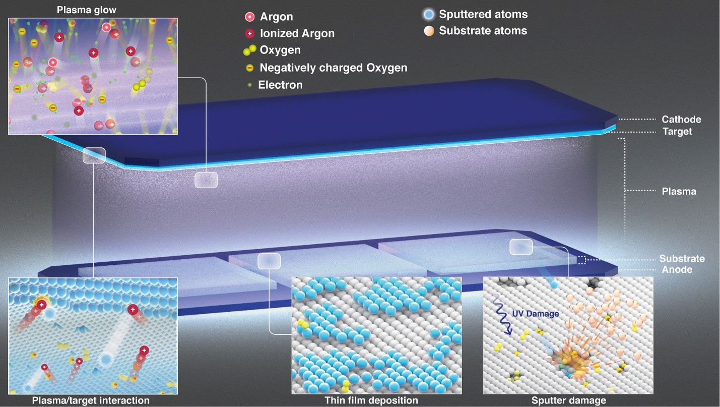
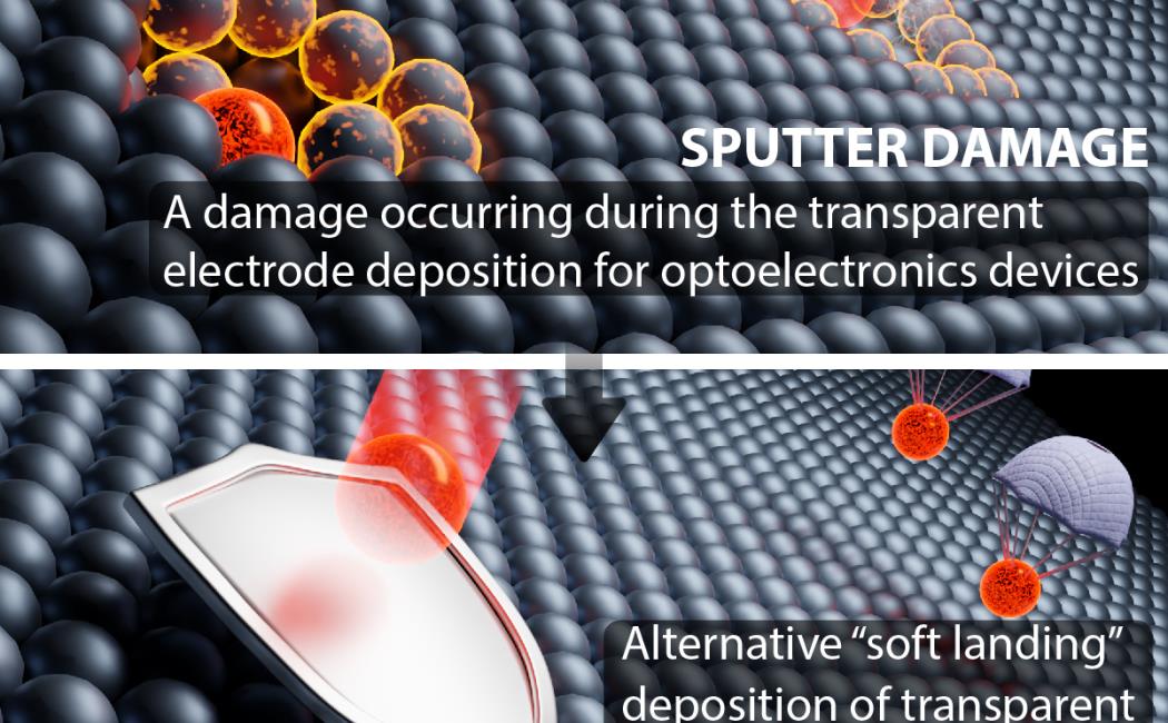
Figure 1. Sputtering process and damage mechanism
Considering the above aspects, Erkan Aydin, Cesur Altinkaya (he was visiting student from Turkey, and now he is a Ph.D. student at KPV-Lab), and Stefaan De Wolf worked with researchers from KAUST Solar Center, University of Twente (The Netherlands), and Universidad de Valencia (Spain) to elaborate the sputtering damage, its mitigation strategies and future directions for solar cells and LEDs to increase the device performances. The review, published in Matter, describes sputtering and damage mechanisms in detail, elaborates the protection methods in the literature, i.e., buffer layers, and shows alternative techniques, called soft landing, which can compete with sputtering.
Dr. Erkan Aydin, a research scientist from the KPV Lab and lead author, says, “There are hidden problems behind the scene of smoothly working optoelectronic devices, one of them is sputter damage, we give a comprehensive understanding of sputter damage, usage of transparent thin films and buffer layers, and alternative soft-landing methods in this review. To do so, we intensely were benefitted from our individual lab experiences with international collaborators to be able to give reasonable and applicable directions for researchers.”
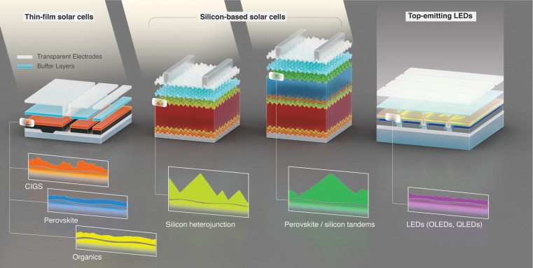
Figure 2. Device sketches of different device technologies and their surface morphologies.
The ideas presented in this review is valid not only for the fields of solar cells and LEDs but also they can easily be extended for other nanotechnology applications suffered from sputter damages; therefore we believe that this review may be a guide for researchers around the globe to deal with detrimental consequences of harsh deposition techniques,” says Prof. Dr. Stefaan De Wolf, the lead author of the publication and head of the KPV-Lab.
Reference: Erkan Aydin, Cesur Altinkaya, Yury Smirnov, Muhammad A. Yaqin, Kassio P.S. Zanoni, Abhyuday Paliwal, Yuliar Firdaus, Thomas G. Allen, Thomas D. Anthopoulos, Henk J. Bolink, Monica Morales-Masis, Stefaan De Wolf, Sputtered transparent electrodes for optoelectronic devices: Induced damage and mitigation strategies, Matter, Volume 4, Issue 11,2021, https://doi.org/10.1016/j.matt.2021.09.021.