15 April, 2020
Perovskite/silicon tandem solar cell is an emerging photovoltaic technology since it promises efficiency values beyond the single-junction limits of the silicon solar cells at competitive prices. Nowadays, several groups have reported power conversion efficiency values >25% for lab-scale devices (~ 1cm2) and since several years Oxford PV is developing such solar cells aiming a large scale deployment.1-7 So far, most of the reported perovskite/silicon tandem solar cells are in the p-i-n configuration owing to their ease of processing, readily available efficient rear-side emitter silicon heterojunction devices, etc.
In the p-i-n configuration, the p-type contacts are interfacing with recombination layers, which is ITO in most of the reports. For the p-type, hole-collecting contacts, there are several options in literature such as PEDOT: PSS, PTAA, Spiro-TTB, Poly-TPD, CuSCN, CuO, CuPc, CuI, etc. So far, the most efficient HTLs on the front side flat tandem is PTAA. Front side planar devices are preferred due to the easiness of transferring the already developed knowledge on the planar glass substrates.
On the other hand, utilizing textured bottom cells improves the light-capturing in the bottom cells by increasing the near-infrared response, and enables efficient charge extraction.1 In addition, textured bottom cells bring industrial relevance to the tandem solar cells since it simplifies the process and reduces the wafer preparation cost. However, well-established solution-based material systems often fail on textured substrates. The main issue with solution processing is the lack of conformal coverage on the rough surfaces. At this point, sputtered NiOx stands out as a promising alternative due to the following advantages.
In our recent study in Science Magazine, together with the Sargent Group from the University of Toronto, we successfully demonstrated these advantages with 25.7% power conversion efficiency by utilizing the RF-sputtered nanocrystalline NiOx hole transport layers on textured interfaces.
Currently, RF-sputtered nanocrystalline NiOx hole transport layers are a well-established baseline process at KPV-LAB for the single-junction perovskite and perovskite/silicon tandem solar cells. Recently, our research team is working to passivate the interfacial defects between perovskite and NiOx layers utilizing various passivation routes for further performance enhancement.

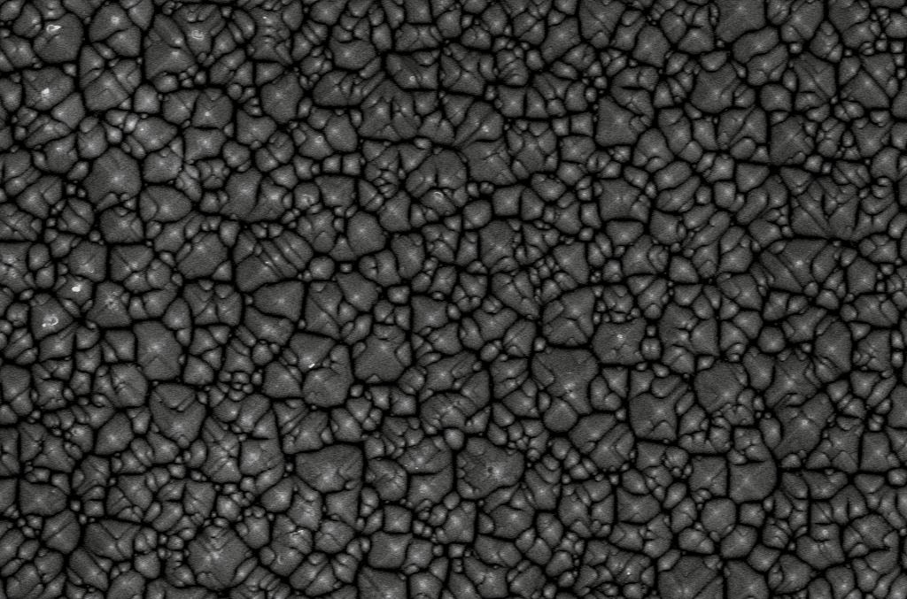
Figure. NiOx thin films on the pyramidal textured 6-inch silicon device (blue colored layer). SEM cross-section images confirm the conformal coating even the top of the pyramids and end of the valleys.
To read more about the processing and the properties of the room-temperature sputtered NiOx layers, the following publications can be visited.
References