

08 May, 2019
Metal‐halide perovskites are rapidly emerging as an important class of photovoltaic absorbers that may enable high‐performance solar cells at an affordable cost. Thanks to the appealing optoelectronic properties of these materials, tremendous progress have been reported in the last few years in terms of power conversion efficiencies (PCE) of perovskite solar cells (PSCs), now with record values in excess of 24%.
.png?sfvrsn=4f27cd63_2)
Figure. NREL best research-cell efficiencies chart which is showing the fast progress of the perovskite solar cells. (Reference: https://www.nrel.gov/pv/cell-efficiency.html)
Nevertheless, the crystalline lattice of perovskites often includes defects, such as interstitials, vacancies, and impurities; at the grain boundaries and surfaces, dangling bonds can also be present, which all contribute to nonradiative recombination of photo‐carriers. On the device level, such recombination undesirably inflates the open‐circuit voltage deficit, acting thus as a significant roadblock toward the theoretical efficiency limit of 30%.

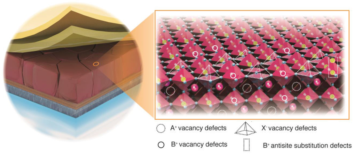
Figure. Schematic illustration of typical PSCs and detailed view of possible surface defects on perovskite crystals, e.g., interstitials, substitutional, and vacancies. (Reference: E. Aydin et al., Advanced Materials, 0, 1900428.)
Herein, the focus is on the origin of the various voltage‐limiting mechanisms in PSCs, and possible mitigation strategies are discussed. Contact passivation schemes and the effect of such methods on the reduction of hysteresis are described. Furthermore, several strategies that demonstrate how passivating contacts can increase the stability of PSCs are elucidated. Finally, the remaining key challenges in contact design are prioritized and an outlook on how passivating contacts will contribute to further the progress toward market readiness of high‐efficiency PSCs is presented.
To see the full paper please click.